An 8.91 nW, 1.74 ppm/°C Subthreshold CMOS-Only Voltage Reference for Temperature Sensors
Abstract
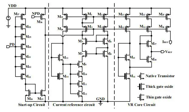
This paper presents a low-power CMOS voltage reference (VR) based on a two-stage stacked diode-connected MOS transistor (SDMT) structure, implemented entirely with MOS transistors. The VR is designed using a standard 0.18 μm CMOS process and occupies an active area of 0.029 mm2, with all transistors operating in the subthreshold region. Post-layout simulations show that the reference voltage reaches 365 mV at 27 °C, while the power consumption is only 8.91 nW. The VR exhibits a temperature coefficient of 1.74 ppm/°C across a wide temperature range from −40 °C to 125 °C. In addition, it demonstrates a line sensitivity (LS) of 0.25 %/V over a supply voltage range of 0.7 V to 1.8 V, confirming its excellent stability and ultra-low-power performance for temperature sensor applications.
Bingjun Xiong
PhD Student
My research interests include circuit design of optical receivers and references.
Feng Yan
PhD Student
My research interests include circuit design of analog front end for biomedical applications and sensor interfaces.
Kangkang Sun
PhD Student
My research interests include circuit design of analog to digital converter for biomedical applications and SAR ADC.
Zhipeng Li
PhD Student
My research interests include circuit design of image sensors and energy harvesting circuits.
Jian Guan
PhD Student
My research interests include the design of solar cells and energy harvesting circuits.
Jingjing Liu
Associate Professor
My research interests include low-power smart micro-sensor integrated circuit design, image sensors, biomedical sensors, and energy harvesting circuits.